English
Blog

Blog

Working hand in hand with global customers to lead the future of intelligent manufacturing together.


Further Discussion on Setting the Lead-Free Reflow Soldering Temperature Profile

2026-08-17

In terms of backward compatibility, some components have only undergone lead-free surface treatment. For component suppliers, it is not cost-effective to provide both tin-lead and lead-free versions of the same component.

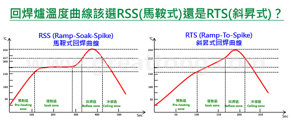
PCBA Lecture Hall: Should the reflow oven temperature curve use RSS or RTS type?

2026-08-17

Should the reflow temperature profile be set to the RSS type (saddle type) or the RTS type (ramp-soak-spike type)? TESDATA has found that many PCBA engineers are constantly troubled by this question, because some bosses require using RTS, but they themselves feel uneasy about it.

Discussion on Technical Requirements for Through-Hole Reflow Soldering

2026-08-17

Pin-in-paste reflow soldering is an emerging technology in international electronic assembly applications. When a PCB has both surface-mount components and a small number of through-hole components such as sockets on the same side, we typically adopt the approach of first placing the surface-mount components through the reflow oven, then manually inserting the through-hole components and passing them through wave soldering. However, if pin-in-paste reflow soldering technology is used, it is only necessary to insert the through-hole components after the surface-mount placement is completed and before entering the reflow oven, and then pass everything through the reflow oven together.

CSP and Flip Chip Assembly with No-Clean Flux (Part 3)

2026-08-17

Table 1 contains the calculated safety margins and placement accuracy for the flip chips used in the experiment, with three different solder mask thicknesses. Table 1, calculated safety margins and placement accuracy Solder ball diameter 190 microns? Solder mask opening 190 microns Solder mask opening 160 microns Solder mask thickness (microns) Safety margin (microns) Placement accuracy (microns) Placement accuracy (microns) 53065501042533815514429? ????For flip chips with fiducial points defined by local solder mask openings and landing pads defined by the solder mask, the conclusion is: . Under the solder ball diameter, minimum solder mask opening, and solder mask

CSP and Flip Chip Assembly with No-Clean Flux (Part 2)

2026-08-17

After placement, the board is soldered and the components undergo electrical testing. The daisy-chain measurement results are shown in Figure 2 with a blue dash-dot line. The theoretical tolerance positions of the solder mask are also indicated in the figure. ? The three theoretical regions are: ?. A consistently good, safe region, corresponding to the copper pad or soldering area. . A transition region, which is the tolerance area of the solder mask; but when placement occurs here, soldering will depend on the position of the solder mask. . A consistently faulty region, which exceeds the tolerance limits of the solder mask; connections in this area are not soldered. ? Measurements from several boards show that the position (tolerance) of the solder mask is not always consistent and may

CSP and Flip Chip Assembly with No-Clean Flux (Part 1)

2026-08-17

This article describes how a recent research project discovered how component spacing and board layout affect the placement accuracy of CSP and flip chips.

Warning: session_start(): Session cannot be started after headers have already been sent in /www/wwwroot/hym.com/includes/class.admin_language.php on line 139
💬
在线客服
在线
对方正在输入...
您有任何问题可以咨询我们